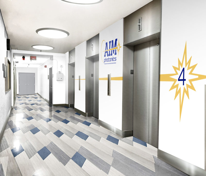
AIM Photonics TAP Facility Headquarters
Accessible facility for integrated silicon photonics test, assembly, and packaging.

AIM Photonics is a consortium of academic, government and business entities focused on advancing US photonics manufacturing capabilities. Their Test, Assembly, and Packaging (TAP) Facility occupies the 4th and 5th floors of ON Semiconductor, which were gutted for new offices, labs, conference center, and cleanrooms. The building was structurally reinforced to bear the weight of $40M in new manufacturing equipment and tools, with modernized infrastructure to meet new high-tech needs.


